Tuesday, January 29, 2019

Common resolutions in the market (camera and home theater)

Compare Resolutions


¼ HD and WXGA resolution comparison


Ref: https://www.projectorpeople.com/resources/resolution-guide.asp


This chart shows the most common display resolutions, with the color of each resolution type indicating the display ratio (e.g. red indicates a 4:3 ratio).


Ref: https://en.wikipedia.org/wiki/Display_resolution

Methods to reduce 1/f noise

1. Use a larger gate area WL, which has less flicker noise. Since often the op-amp input devices dominate the noise, these should have large gate areas.

2. PMOS devices have considerably smaller values for the constant K than the NMOS ones. So PMOS transistors are preferred in the design.

3. Correlated double sampling at the opamp input may store some noise and then subtracted from the signal. This introduces a highpass filtering of the noise and suppresses it effectively at frequencies which are much lower than the sampling frequency.

4. Chopper stabilization can be used to modulate the 1/f noise out of the signal band.

Friday, January 25, 2019

Interesting Features related to ADE L

1. The best size of ADE window is 700 pixels wide by 450 pixels high.

2. The variables can be edit in place by selecting the name and click in the value field to edit it.

3. The outputs can be check or uncheck the plot and save directly from the main window.

4. VAR parameterization is a good function to help you create and use design variables just about anywhere in your simulation setup. For example, you can specify the transient analysis stop time by putting VAR("stopTime") in the appropriate field in the choosing analyses from. This will automatically create a design variable which you can change directly from the main window. Similarly, you can parameterize model files and sections, simulator options and many other things.

5. Plot refresh can allows you to control the behavior of ViVa graph windows when you re-run a simulation. If you chose to auto-plot waveforms, any modification you made to your graph windows were wiped out when you re-ran the simulation.

Thursday, January 24, 2019

How many points for ADC INL/DNL Histogram Simulation

The histogram test method is to apply slow linear ramp to the ADC and derives the DNL and INL directly from a total number of occurrences of each code at the output of the ADC.

How is the ramp slope? And how many points do we need for each digital code?

For example, if the ADC sampling rate is 1MHz. So every 1us we can get one sample. The LSB is 1mV. It has a 10-bit resolution.

To get 0.01LSB measurement resolution, we need 100 samples/code.

The total simulation time is 1us * 100 * 2^10=102.4 ms.
The ramp slope is 10uV/us.

Tuesday, January 22, 2019

Additional cadence design libraries for IC design

Cadence provides many design libraries.


libmgr


Cadence also provides "Customizing the Library Manager"
The actual method is quoted as below:
"At first, create a dummy directory with the name you want to give your combined library (kind of a kludge, but oh well).  Then edit your cds.lib and add 2 lines:

DEFINE <combinedLibName> <pathToDummyDirectoryYouCreatedAbove>

ASSIGN <combinedLibName> COMBINE <lib1> <lib2> ...

These lines need to go after all the lib1, lib2, etc. libraries are defined.

That's it.  Now when you open the Library Manager, you'll see your combined library name with a "+" sign next to it.  If you click on the combined library name, you'll see all the cells in all the libraries combined.  If you click the "+" sign, you can still access the libraries individually as usual. "

Matlab toolbox for IC design


  • CSATOOL to help design a switched-capacitor DAC for an SAR ADC


Continue ...


Open-source Online Tools


  • Programming online for verilog/systemverilog/python/c++


  • Table Online Creator for LaTex/HTML/MARKDOWN


  • Math Equation Online Creator for HTML


  • Free Photo Cloud Storage (html code can be embedded in Blogger)


capacitor consideration in switched-capacitor DACs

In the capacitor array of a switched-capacitor DAC, each capacitor can be expressed as below considering mismatch and parasitics;


where  is the parasitic capacitance related to the i-th capacitor and  is the mismatch equivalent capacitance affecting the unit capacitor. The effect of the parasitic capacitances can be considered deterministic, depending on layout inaccuracies, capacitor geometry, and wirings. On the contrary, the capacitance mismatch can be modeled as a Gaussian distribution of the unit capacitor value with a mean equal to the nominal capacitance, , and a standard deviation equal to 


where  being the Pelgrom mismatch coefficient, the unit capacitance, the area and the unit capacitance per area, respectively.

For example, if the Pelgrom mismatch coefficient is given as 0.43% um, for a 22fF unit capacitor with 3um x 3um area, the unit capacitance per area is 2.45fF/um^2 and the standard deviation is  0.02237fF.

Another important parasitic in the charge-redistribution array is the stray capacitance connected to the top-plate node of the array to a fixed voltage node. The parasitic capacitance causes a gain error in the converter characteristic but in some ADC topologies, it can also affect the converter nonlinearity.

The maximum standard deviation of the DNL in a conventional binary weighted array with single-ended input is


In order to get less than 1LSB DNL, the unit capacitor needs to be


Using the above parameters, a 10bit DAC needs to have a larger than 733fF unit capacitor to guarantee the DNL less than 1LSB.

Ref[1] mentioned that overall limitations and a suitable margin suggest using a unit capacitor in SC DACs to be larger than 40fF.

Hence, interesting research could study how the size of capacitors in DAC affects its linearity.


[1] Design of an ultra-low power SA-ADC with medium/high resolution and speed written by Andrea Agnes, and et al. 

Monday, January 21, 2019

ADC main parameters

ADC signal-to-noise and distortion ratio (SNDR or SiNAD)


Total Harmonic Distortion(THD)


Where V2, V3,...Vn are the magnitude of harmonic distortions. Higher frequency will have less magnitude, which is less than the noise floor or is beyond the bandwidth of interest. Data sheet typically specifies to what order the harmonic distortion has been calculated. For example, up to the fifth harmonic is common. 

Signal-to-noise ratio (SNR)


ENOB


For testing ADC, a near full-scale input signal (the preferred input-tone amplitude is -0.5dBFS to -1dBFS) is applied, which avoids the situation of overdriving the quantizer. For the full-scale input, ENOB is expressed:


If the input signal is less than full-scale, like -0.5dBFS (expressed in dB related full scale), the ENOB is expressed:


Clock Jitter
Figure 2
High-speed high-resolution ADCs are sensitive to the quality of the clock input. To achieve superior SNR in a high-speed ADC, the RMS clock jitter must be carefully considered, based on the requirements of the applications' input frequency. 

Figure 6
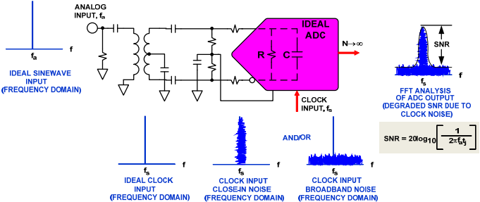
Clock jitter limited SNR can be plotted against the analog input frequency for various clock-jitter profiles
Faster input frequency needs smaller clock jitter to obtain the same SNR. For example, an rms clock jitter of 200fs limits an ADC's SNR performance to no better than 70dB at 250MHz. However, a 1GHz input signal would need an rms clock jitter of 50fs or better to achieve the same SNR performance of 70dB. 

SAR ADC design consideration

A typical SAR ADC consists of three components: DAC, comparator, and SAR logic. It has become a superior ADC topology with a good tradeoff between power consumption, speed, and resolution.

Many studies have been made in several aspects. The first one is related to DAC topology. There are three main structures: switched resistors network, switched current sources network, and switched capacitors network. Among them, two main categories of Switched-capacitor DACs are charging-sharing and charge-redistribution. Many scholars made efforts on proposing and discussing different types of SC architectures and switching algorithms to improve the efficiency, linearity, accuracy and power consumption.

The second one is related to comparator design. The dynamic comparator has been dominant for good power efficiency. Inverter-based and time-based comparator have been popular recently.

The third one is related to SAR logic. The switching method can be accounted for this aspect. The SAR logic also plays a role in outputting digital codes. When the CMOS processing keeps scaling, the digital power of the SAR logic becomes more dominant in the whole SAR ADC. So to find a better way of saving digital power could be a promising research direction.

In addition, people also study the non-binary search, binary search with redundancy, and calibration method to optimize the linearity, mismatch and gain error issues for the SAR ADC architecture.


The SC DAC network doesn't consume static power so it is widely used for low power applications. Another reason is that SC network can be used as S/H circuit in the sampling phase.

In terms of SC DAC, many studies have been made on capacitor array topologies and switching methods. Some parameters like ADC linearity, energy efficiency, performance, and area are used to evaluate them.

The split capacitor topology is one of them, which aims to reduce the capacitor area. However, considering the capacitor mismatch, parasitic capacitance, kT/C noise, the split capacitor topology is more sensitive to parasitic effects, a larger unit capacitor must be used and in some cases can produce even larger total area than simply binary-weighted capacitor network.


Charge-redistribution SAR ADC vs Charge-sharing SAR ADC

Nowadays the majority of SAR ADCs are implemented in charge-redistribution (CR) topology. Charge-sharing (CS) principle turns out to be an alternative approach.

One important distinction between CR and CS SAR architectures is the shape of the current drawn from the reference voltage. The CR SAR interacts with the reference source at each bit decision cycle, the CS SAR draws all the charge required for conversion from VREF in a single cycle and performs the charge processing passively. So CS SAR ADCs ease the requirements of the reference generation circuit.

However, the CS ADC is more susceptible to comparator and noise and offset, because the latter causes non-linearity in the ADC transfer curve. In CR ADCs, comparator offset brings only an offset in the transfer curve.


Sunday, January 20, 2019

Open Loop Cascade of amplifiers


N ωN/ω1 |AV(0)|
1
1
10000
2
64.36
100
3
236.64
21.54
4
434.98
10
5
611.16
6.31
10
1066.55
2.51
20
1184.87
1.58

For a given voltage gain, cascade structure could lower each stage gain requirement and enlarge the final amplifier's bandwidth.

Friday, January 18, 2019

Table to show noise of capacitors in room temperature

Noise of capacitor at T=300K
Capacitance
(fF)
sqrt(kT/C)
rms noise
(uV)
peak to peak noise
(uV)
1 2034.698995 13429.01337
10 643.4283177 4246.626897
20 454.9725266 3002.818676
40 321.7141588 2123.313448
50 287.7498914 1899.149283
60 262.6785107 1733.678171
100 203.4698995 1342.901337
120 185.7417562 1225.895591
150 166.1324773 1096.47435
240 131.3392554 866.8390854
1000 64.34283177 424.6626897

Table to show required settling time for a ADC with different resolutions


number of bits 0.5LSB Time Constant (k) multiplier Time Constant (k) multiplier
8 0.1953125% 6.2 6.9
9 0.0976563% 6.9 7.6
10 0.0488281% 7.6 8.3
11 0.0244141% 8.3 9.0
12 0.0122070% 9.0 9.7
14 0.0030518% 10.4 11.1
16 0.0007629% 11.8 12.5
18 0.0001907% 13.2 13.9
20 0.0000477% 14.6 15.2
22 0.0000119% 15.9 16.6
24 0.0000030% 17.3 18.0
1/2 LSB settling accuracy 1/4 LSB settling accuracy

If some one needs to the excel file to save a copy in a personal computer, please use the following link to download: google sheet document

Timing characteristics of an A/D converter

Three timing terms are important in every A/D converter.

  • acquisition time: it is the time needed for the input signal to be connected to the internal capacitor of the ADC and store its voltage on the internal sampling capacitor. 

  • conversion time: it is the time of the ADC to complete the digitization process through several comparisons. 

  • throughput rate: it is also called sampling rate. It means the maximum frequency at which A/D converter can be repeated. 

Thursday, January 17, 2019

How to simulate setup time and hold time of any DFF in cadence tool

Setup time is defined as the minimum amount of time before the clock's active edge that the data must be stable for it to be latched correctly. Any violation may cause incorrect data to be captured, which is known as setup violation.

Hold time is defined as the minimum amount of time after the clock's active edge during which data must be stable. A violation in this case may cause incorrect data to be latched, which is known as a hold violation. Note that setup and hold time is measured with respect to the active clock edge only.


enter image description here
Many fresh engineers know the definition but they don't know how to simulate them. I wrote a tutorial summarizing previous works coming from excellent engineers. 

The tutorial discussed how to simulate the setup time and hold time of a DFF.

Wednesday, January 16, 2019

Tips and Tricks on Virtuoso Visualization and Analysis XL Markers by Cadence

A marker is basically a label used to attach a description to a point on the trace, and by default displays the X and Y coordinates of its intersection with the trace. With the help of markers, you can view and analyze the specific points or areas on the trace and perform further analysis. You can also use the markers to represent expressions. Markers can be of various types, such as point, vertical, horizontal, AB, delta, and so on. Let us have a quick look at the picture below to get an idea of how markers look. In this picture, the trace contains the point (M1), vertical (V1), and horizontal (H1) markers.  

Here is a list of some useful bindkeys that you can keep handy:
  • M, V, H: Creates a point, vertical, and horizontal marker, respectively.
  • Q: Opens the marker properties form that you can use to change the various attributes of a marker, such as label, position, intercepts, significant digits, notation, and so on.
  • N, P: Moves the marker to next or previous points on the trace based on the snapping criteria selected in the Next/Prev Snap Point drop-down available in the marker properties form. The default snapping criteria is Data Point. The other available options are—Local Maxima, Local Minima, Local Max or Min, Specific Y Value, Specific X Value, Global Maxima, and Global Minima. I must say it’s really an interesting and useful feature and comes handy when you want to analyze specific values on the trace.
  • Shift+D: Creates a delta marker between two or more markers: It’s interesting to note that you can mix point, vertical, horizontal marker and get delta values from a point to a line.
  • D: Creates a chain of delta markers. Select a marker and wherever on the trace you press the bindkey D, you will get a marker of the selected type and a delta value between them.
  • Ctrl+E:  Deletes all the markers at one go. It acts like a savior when you have lots of markers added on the graph. Moreover, if you have delta markers added on to the graph, you can hide their child labels to make the graphs look neat. 
  • Drag-and-Drop
Well, it is not a new feature for graphs, but a very convenient one! It’s helpful when you want to instantly view the marker intercept values at different locations on the trace. Undoubtedly, you can also change the intercept values through the marker Properties form, but you need to perform a series of steps to do that.
  • Context-Sensitive Menu
Right-click a marker and use the context-sensitive menu options to perform certain marker-specific tasks, such as change the marker properties, snap the marker to the next or previous edge, delete the marker, and so on.
  • Horizontal and Vertical Marker Tables
Use these assistants to view the intercept values of all the horizontal or vertical markers added on to the graph. To open these assistants, choose WindowAssistantsVert Marker Table or Horiz Marker Table. Alternatively, right-click anywhere on the menu bar and open these assistants from the context-sensitive menu. The one thing I like about these assistants is they act as 'one-stop shop.'
  •  Special Marker (AB)

We call it an AB Marker! This is a special delta marker of type XY and helps view the dx, dy, and slope values between two points on the same or different traces. Note that a graph can contain only one AB marker. To create another pair, you need to convert the AB marker into a normal delta marker.


You can use the Markers menu any time to create and work with markers. Here are some useful tips, tricks, and shortcuts that you can use and apply to make the tasks faster and improve productivity.

Tips to use cadence environment in Linux/Unix system

Make Nautilus (file manager) behave like a browser

Nautilus is the default file manager on the lab computers. You have likely noticed that, with the default settings, it spawns a new windows each time you open a folder. If you find this annoying, you can change its behavior with the following steps:
  • Open the preferences dialogue (Edit->Preferences)
  • Click on the behavior tab
  • Tick the always open in browser windows option

Firefox profile lock (error message with "Firefox is currently running...")


Frequently, if you do not close firefox properly, it will give an error message next time you try to open it. To fix this problem, navigate to ~/.mozilla/firefox and look for a folder with a mix of numbers and letters followed by "Default User". In this folder, you will find an invisible file called .parentlock; delete this file and the problem should be fixed.

Locked Files in Cadence

If you try to open an old file and Cadence says you can't edit the file, it is because this file has become "locked." This usually happens as a result of Cadence crashing while the file was open.
To unlock the file, you need to search for and remove (using the rm command) a file that ends in ".cdslck". You will often have to look through directories and subdirectories to find this file, but look in directories that have the same name as the cellview in question. For example if you are having trouble opening the schematic in cellview "Inverter" in library "myLib" then you would go to the folder myLib/Inverter/ and look for all files ending in ".cdslck".
As an alternative to manually searching through the directories you can use the command (from the directory where you start cadence):
find . -name "*.cdslck"
Before you run this command close all open shcematics and layouts. Then simply remove all files that appear.
To remove all cdslck files, you can use the command rm together with searching(from the directory where you start cadence):
find . -name "*.cdslck" -exec rm -f {} \;

Reference: https://secure.engr.oregonstate.edu/wiki/ams/index.php/Cadence/TipsAndTricks#toc11

Set # of sig figs on schematic annotation

Sometimes the number of significant figures on schematic annotations (node voltages, for example) is very high and it becomes difficult to read. To fix this, type the following into the icfb window:
envSetVal("auCore.misc" "labelDigits" 'int 5)
Change the number 5 to your desired number of sig figs. To make this change permanent, add the line to your ~/.cdsenv file.


Set the default script/veriogA editor in Cadence to gedit

  • Option 1: type the following in CIW command line
editor="gedit"
  • Option 2: add the line to .cdsinit
editor="gedit"


Change Waveform Graph windows default settings

Add some of the following lines to .cdsenv file to change the window size, background/foreground color, font size, line thickness,and etc.
;width
viva.graphFrame width string "900"
;height
viva.graphFrame height string "700"
;background color
viva.rectGraph background string "white"
;foreground color
viva.rectGraph foreground string "black"
;axis font
viva.axis font string "Fixed [Misc],14,-1,5,50,0,0,0,0,0"
;marker font
viva.pointMarker font string "Fixed [Misc],14,-1,5,50,0,0,0,0,0"
viva.horizMarker font string "Fixed [Misc],14,-1,5,50,0,0,0,0,0"
viva.vertMarker font string "Fixed [Misc],14,-1,5,50,0,0,0,0,0"
viva.multiDeltaMarker font string "Fixed [Misc],14,-1,5,50,0,0,0,0,0"
viva.refPointMarker font string "Fixed [Misc],14,-1,5,50,0,0,0,0,0"
;line thickness
viva.trace lineThickness string "thick"
You may also use envSetVal to set the environment. For example, to set the background to white, type the following in the CIW window.

envSetVal(“viva.rectGraph” “background” 'string “white”)

Save operating point information over a DC sweep

You may notice that DC operating point information (gm, gds, etc.) does not get saved over a DC sweep. One way to work around this is to replicate the sweep using the parametric sweep tool. In some cases, however, this may constrain your simulation setup. If you simply want the op information to be saved for every point in a sweep, follow these directions:
  • Make a new text file (saveop.scs, for example) in a directory to which you have read-write access.
  • Add the following line to the file, replacing N0 with the name of the device whos operating point you wish to save:
save N0:oppoint

  • Save the file. Return to your ADE window, navigate to Setup->Model Libraries; now the file you just made to the list.
  • Run your simulation and find the saved data in the Results Browser (under the Tools menu in the ADE). You can also access the data with equations (i.e. getData("M0:vdsat" ?result 'dc)).
  • You can, of course, have multiple lines in the file for multiple devices. For large simulations, consider saving disk space by modifying the file to save only the parameters of interest (i.e, N0:gm). More information about the save command can be found in the spectre documentation or by running spectre -h save at the terminal.

Thursday, January 10, 2019

Calculate Copper resistance related to its thickness

Bypass capacitor's purpose

Those on-board ICs with high-speed demand sharp spikes of transient current that the power supply cannot deliver. Power supplies are designed to supply a level amount of power across the entire board, rather than short bursts. To solve this issue, a bypass capacitor can be placed near the IC to supply the required current for these quick spikes. A bypass capacitor does this by storing power and then discharging it to the IC when it requires excess current. This gives the power supply time to respond. Following the spike, the bypass capacitor is recharged and ready for the next cycle.

Bypass capacitors are also important for reducing the ground bounce that comes from digital devices that have faster switching times. Bypass capacitors are also used to filter the low-frequency noise caused by the power supply and are helpful with other signal integrity and EMI issues as well.

How many bypass capacitor needed?

The number of bypass capacitors needed for design will depend in relation to the parts that they are assigned to, and how many of those parts are being used. Bulk capacitors in the 10uF range are usually for each voltage drop on the board. They should be positioned where the voltage is developed or where it enters the board. On some devices, they are used in conjunction with high-speed bypass capacitors.

In general, at least one high-speed bypass capacitors in the 0.1uF range should be placed by each IC. They should be placed as close as possible to their respective IC to supply current immediately. I recommend that devices with multiple power pins should have at least one bypass capacitor for each power pin. Although this will use up more board space, it can significantly help to reduce ground bounce.

The high-speed bypass capacitor can be underneath the device on the opposite side of the board, or just off the pins that the bypass capacitor is connected to on the same side of the board.

For circuits requiring multiple bypass capacitors placed near the power pin of a specific device, the capacitors should be placed next to that pin in ascending order of value. For instance, if both a 0.01uF and a 10uF capacitor are specified for a specific device, place the 0.01uF closest to the device with the 10uF outboard of that. In this way, the larger bulk capacitor will recharge the high-frequency capacitor that is closest to the device pin.

When routing a bypass capacitor, you should start from the power or ground pin of the device and go directly to the capacitor pin. From there the route can continue on a via connecting it to the power or ground plane. You should also use a short and wide traces as possible to connect the bypass capacitor, and use as many vias to connect to the power or ground plane as possible.