Thursday, December 13, 2018

Transfer Altium Design schematic and pcb layout to KiCAD version

Sometimes you don't have license of Altium but you need to review the Altium PCB design. There is a good solution for you to use open-source PCB tool, KiCAD.

But you need to use visit the external tools in KiCAD web and download the altium2kicad one.

Clone or download the package of altium2kicad tool.

Create a new folder: tutorial. Put all the altium2kicad files into tutorial folder.


Install a perl tool: strawberry perl for windows.

Put those altium schematic and layout files into the tutorial folder.


Right click to run the perl script "unpack.pl" and then it unpacks .PcbDoc and .SchDoc files into sub-directories.


Right click to run the perl script "convertschema.pl" to convert .SchDoc to .sch which is readable by KiCAD.


Right click to run the perl script "convertpcb.pl" to convert .PcbDoc to .kicad_pcb which is also readable by KiCAD.

Now the transfer operation is done. You can launch KiCAD and click Browse --> open local File...
Open the .sch or .kicad_pcb files.


Don't delete -cache.lib files which provides lib details for the design.


Thursday, December 6, 2018

ADC basics

The McGill Physiology Virtual Lab provides a good post talking about some basics of Analog-to-digital converters including sampling, resolution, saturation, sampling rate and aliasing, etc.

Tutorial about pipelined adc design

Pipelined ADCs are common used for high-speed high-resolution data acquisition. Dr. Imran Ahmed posted a good tutorial to briefly talk about 1.5bit/stage pipelined adc design as well as addressing some key tradeoffs.

Friday, November 16, 2018

"Ayar Labs: Faster I/O" BY: KEVIN FOGARTY in Semiconductor Engineering

Startup AyarLabs is using a combination of high-bandwidth fiberoptics, low-cost CMOS fabrication and careful target selection to strike efficiently at the datacenter’s worst bottleneck.

“Moore’s Law only covers the processor, not how we move data in and out of it during processing or how to get the processor and memory working at the same speed,” according to Alexandra Wright-Gladstein, co-founder and CEO of Ayar Labs. “We are developing optical transceivers, but we’re very focused on chip I/O , not optics per se. We have a high-efficiency optical-electrical conversion engine with a very small footprint, so our optical devices are tiny. We build it using ordinary CMOS design and fabrication and focus on efficiency, so we end up with a product that uses 10 times less power than any commercial optical transceiver, whether silicon-based or traditional.”

The company is a spin-out from a 10-year MIT research project that developed a dual-core RISC-V architecture chip with 70 million transistors,850 million photonic components, 1MB of RAM, and a fiber I/O port theoretically capable of sending at at 550 Gb/sec and receiving 900Gb/sec.

When the team combined two chips, one serving a processor, the other as memory, they were able to pass data at 2.5Gbit/sec in each direction, expanding bandwidth as needed by adding wavelengths from the external laser that provided light to the chips.

The project was partly funded by two DARPA programs, one designed to increase data rates by combining processing with photonics, and another whose focus was on getting the highest number of FLOPS possible from every watt.

A paper describing the result was published in the journal Nature in December, 2015, complete with a video showing how it works.

The SoC approach is designed partly for efficiency and partly to bridge the gap in design and manufacturing between CMOS and photonics products, according to the paper, which also describes the “zero-change” approach to developing photonics using CMOS techniqes and materials in the integration of photonics to avoid the complication of custom fabrication of photonic components.

The 45nm chip was the first designed with an optical I/O. The commercial product is a lot different than the one described in the journal article, according to Wright-Gladstein, but the research version did more than just give co-founders Chen Sun and Mark Wade a chance to pursue their Ph.D.s.

It also brought in some startup capital after Wright-Gladstein entered the nascent company — then called Optibit — in MIT’s Clean Energy Prize competition and brought home both grand prizes, which totaled $275,000. https://www.scientificcomputing.com/news/2015/05/optical-chips-team-develops-way-integrate-fiber-optics-computer-chips

Optics give datacenters tools to retool
Intel’s 100 Gbit/sec silicon photonic network interface gave datacenter architects the opportunity to change the fundamental design of datacenters by eliminating much of the penalty of distance. Minimizing the delay in providing a Google Translation or passing on a Facebook “Like” used to mean larding each individual server with as much memory as possible, and keeping HDD storage in the rack or very close by so that data not stored in main memory didn’t have far to go.

Replacing copper running at 10Gbit/sec, 25 Gbit/sec or even 40Gbitsec with fiber running 100Gbit/sec, while using less energy and generating less heat, allows hyperscale datacenters to pack in even more hardware and delay just a little the need to build a new one. The year it delivered its first photonics product, 2016, was also the first time that cloud service providers bought more Intel chips than Intel’s traditional customers, according to a 451 Research paper about the project.

Sales of silicon photonic switches generated only $30 million during 2016, according to researchers at Yole Développement, but will make up 35% of the market for intra-datacenter communication by 2025, generating sales worth $560 million. Cloud service companies and large data centers are doing most of the spending to increase the bandwidth of rack-top switches, and increasingly to link geographically separate facilities using wave-division multiplexing. WDM sales rose 225% during 2017 compared to 2016, according to analysts at the Dell’Oro Group.

Tuesday, November 6, 2018

Use negative feedback opamp to understand the feedback divider in Phase-locked loop

Phase-locked loop is a feedback system. In the feedback loop, a divider is usually used to get a frequency multiplication.

At the first sight, it is hard to understand why the output frequency feedback with a divider can get a increased frequency clock signal.

I found a article in ALL ABOUT CIRCUITS website. It is very useful to explain it by using the negative feedback opamp knowledge.

In the opamp non-inverting amplifier, if the output signal is connected directly back to the inverting input termal, it is used as a voltage follower, or unity-gain buffer. As a result, the opamp does whatever it needs to do to make the output voltage equal to the input voltage.

What if we need a gain? We just use some resistors to turn the feedback loop into a voltage divider. The feedback voltage, Vfb, will be a division of output voltage, Vout.

As we know, the negative-feedback arrangement causes the op-amp to modify its output with one goal: make the voltage at two input nodes equal. When it is configured as unity-gain buffer, this means the Vout must be equal Vin.

But the voltage divider in the feedback loop changes everything. Now, the voltage at the inverting input is DIV times smaller than the voltage at the output. Thus, in order to make the inverting-input voltage equal to the noninverting-input voltage, the output voltage must be DIV times larger than the input voltage.

With an op-amp, then, we create voltage gain by reducing the amplitude of the feedback voltage; with a PLL, we create frequency gain by reducing the frequency of the feedback waveform. To continue the analogy, the gain of a noninverting opamp circuit is equal to the factor by which the feedback voltage is divided, and the amount of frequency multiplication perfomed by the PLL is equal to the factor by which the feedback signal's frequency is divided.

Friday, November 2, 2018

Fundamentals of Data conversion

I really like a excellent summary about data conversion:
"No matter which ADC and what kind of ADC architecture, they all perform two basic and fundamental operations: discretization in time and discretization in amplitude. "
The first step, time discretization, is also called sampling operation. The continually time-varying input analog signal is sampled at uniformly spaced times at a frequency of fs and the samples are thus separated by a period of T=1/fs.

Although the sampled signal are obtained, they are still has different infinite range of values in amplitude domain. Therefore, we can't be represent them precisely in digital codes.

The second step is to digitize the sampled signal in amplitude. The so-called quantization error limits the resolution of the converter.

There are two broad categories of ADCs: Nyquist-rate and over-sampling converters. They typically offer different compromises between ADC resolution and output sampling rate.

Nyquist-rate converters are those that operate at the minimum sampling frequency necessary to capture all the information about the entire input bandwidth, and therefore the output data rate of a Nyquist-rate ADC can be very high.

Over-sampling converters are sampling at very high frequency. The noise-shaping technique is used to filter the in-band noise and to achieve higher SNDR and SFDR. Two types of over-sampling converters are developed currently, DT and CT. Indeed CT sigma delta ADC is introduced earlier in 1962 than DT sigma delta ADC. But when switched-capacitor circuits were introduced, most CT sigma delta modulators were implemented with DT loop filters. SC circuits remain popular because of their insensitivity to signal waveform characteristics.

In addition, the time constants of SC integrators scale with sampling frequency, allowing for greater system flexibility. However, interest in CT sigma delta modulators has been renewed because of their benefits versus sampled-input ADCs, such as employing lower-power integrator amplifiers and including inherent anti-aliasing filtering.

Because of the over-sampling operation, the output rates of sigma-delta ADCs are currently limited to less than 100MSPS while pipleine ADCs are capable of operating up to 500MSPS and beyond. Indeed, for a given technology, Nyquist-rate converters will always be able to operate faster than sigma-delta ADCs because of the over-sampling necessary in a sigma-delta design. Fortunately, the benefts of CT sigma delta technology outweigh the drawbacks for high-resolution applications at sampling rates below 100MSPS.


Monday, October 29, 2018

Analog CDS vs Digital CDS


Correlated Double Sampling (CDS) is a technique to obtain two samples, reset and signal voltages, which is widely used in CMOS image sensor system to reduce the FPN noise.

There are two types of CDS: analog and digital CDS.
Analog CDS means that the subtraction between reset and pixel voltages is achieved in analog domain.

Digital CDS means that both reset and pixel voltages are converted to digital bits and then subtract them in digital domain.

Friday, October 5, 2018

Purpose of PSS and Pnoise analysis

For static circuitry, small-signal analysis such as AC or NOISE can be used to analyze them and understand their performance in terms of small signal input and noise stuff after giving the DC operating point. The operating point is found by solving the nonlinear device equations for the steady-state of the circuit with large signals, at DC analysis, and then the nonlinear elements are linearized.

However, for dynamic one such switched-cap circuit, the circuitry is working using clock signals. They can't provide a DC operating point since the circuit requires the clock signal to be active to have a steady state. PSS (periodic steady state) analysis of cadence spectreRF could linearize the network at a periodic operating point and PNOISE (periodic noise) can conduct noise analysis on this periodic operating point. 

Wednesday, October 3, 2018

Installation Opensource EDA tools: Magic/XCircuit/IRSIM/Netgen/Qflow/Qrouter

The website: www.howtoinstall.co/en provides installation commands for debian and ubuntu OS.

The open source EDA tools are provided by Open Circuit Design.


Magic : VLSI layout editor, extraction and DRC tool

XCircuit : circuit drawing and schematic capture tool

IRSIM : switch-level digital circuit simulator

Netgen : LVS and netlist conversion tool

Qrouter : over-the-cell detail router

Qflow : complete digital synthesis design flow using open-source software and  
standard cell libraries.
PCB : pcb board design tool 


The tools are installed in Ubuntu 16.04 Virtual Box. Use the following command to install them

Sudo apt-get update

Sudo apt-get install magic

Sudo apt-get install xcircuit

Sudo apt-get install irsim

Sudo apt-get install netgen

Sudo apt-get install qrouter

Sudo apt-get install qflow
Sudo apt-get install pcb

However, those commands have some issues.

For qflow installation, we better use the github link (git://opencircuitdesign.com/qflow-1.1 ) to clone the installation package.

The command lines are
git clone git://opencircuitdesign.com/qflow-1.1
cd qflow-1.1
./configure
make
make install
PS:
1. make sure you install python3.5 and python3.5tk or even higher version like 3.6 or 3.7.
sudo add-apt-repository ppa:fkrull/deadsnakes
sudo apt-get update
sudo apt-get install python3.5
sudo apt-get install python3.5-tk

2. Any missing libraries, please use apt-get install packages_name to install them.

3. After finishing the installation of qlfow, please check whether the directory /usr/local/share/qflow exists or not.

4. For making a tutorial, please make several directories. Then move the verilog file into source folder. Open the tutorial project folder and use command "qflow design_veilog_file" to run the qflow for generating three command files.
mkdir tutorial1
mkdir source
mkdir layout
mkdir synthesis
5. In final, "qflow gui" to launch the GUI window of qflow. "qflow gui&" can also be used.

For not getting compitable issues for different software, please download those packages from OCD and install them, especially magic, netgen, qrouter. Icarus verilog is also helpful to run simulations. Take you time to install it. 

In final, each project will generate a gds file located in layout folder. Please install klayout software to view it.

Monday, September 24, 2018

Cadence APS vs XPS vs AMS


Cadence Spectre APS : Spectre Accelerated Parallel Simulator

Cadence Spectre XPS : Spectre eXtensive Partitioning Simulator

Cadence Spectre AMS Designer : Spectre AMS Designer Simulator

If you want to read the official documents about these three simulators, please visit cadence link.
You can also get a cadence tutorial file named: Spectre Circuit Simulator Reference from Cadence Support.
---

Spectre XPS is a FastSPICE circuit simulator that uses techniques like partitioning in order to simulate large, extracted netlists with 10's of millions of elements, and allowing IR drop analysis for extracted netlists.

Spectre APS is used for smaller designs and for highest accuracy circuits like: BER of an ADC, PLL jitter. It can be used without issues in transient analysis. (More discussions about APS, please email me.)

For introduction of AMS simulator, you can view ECEN 5007 course website of Prof. Hanh-Phuc Le.

Wednesday, September 12, 2018

LiDAR Introduction

In 2018, over $1B is raised by over 70 LiDAR companies. Analysts from Markets and Markets (www.marketsandmarkets.com) forecast the LiDAR market is going to hit 5,204.8 Million USD and will grow at a CAGR of 25.8% from 2018 to 2022. Therefore, the next five years will be a golden age for the automotive LiDAR market. 

Today, let's talk about some basic knowledge about LiDAR.

LiDAR stands for Light Detection and Ranging (sometimes light imaging, detection, and ranging).  It is a surveying method that measures a distance to a target by illuminating the target with pulsed laser light and measuring the reflected pulses with a sensor. Differences in laser return times and wavelengths can then be used to make digital 3-D representations of the target.

Applications
LiDAR has broad applications in geodesy, geomatics, archaeology, geography, geology, geomorphology, seismology, forestry, atmospheric physics, laser guidance, airborne laser swath mapping, and laser altimetry. Nowadays, it is also used in control and navigation for some autonomous cars becoming the world-wide favorite topic both in academic and industry.

If you would like to know more about history and general discussions about LiDAR, please visit LiDAR Wikipedia page.

Related image
Image of a rotating LiDAR unit from Renishaw.
In this article, the automotive LiDAR sensor is talked, especially focusing on receiver part. The recent hot topics and research limitation will also be mentioned. LiDAR sensor is used as assistance system for a driver. The challenge is to ensure that it will function under all possible environmental conditions (temperature, solar radiation, darkness, rain, snow), and above all, recognize objects up to 300 yards away. And of course, all this in large-scale production at the lowest possible cost and smallest dimensions.

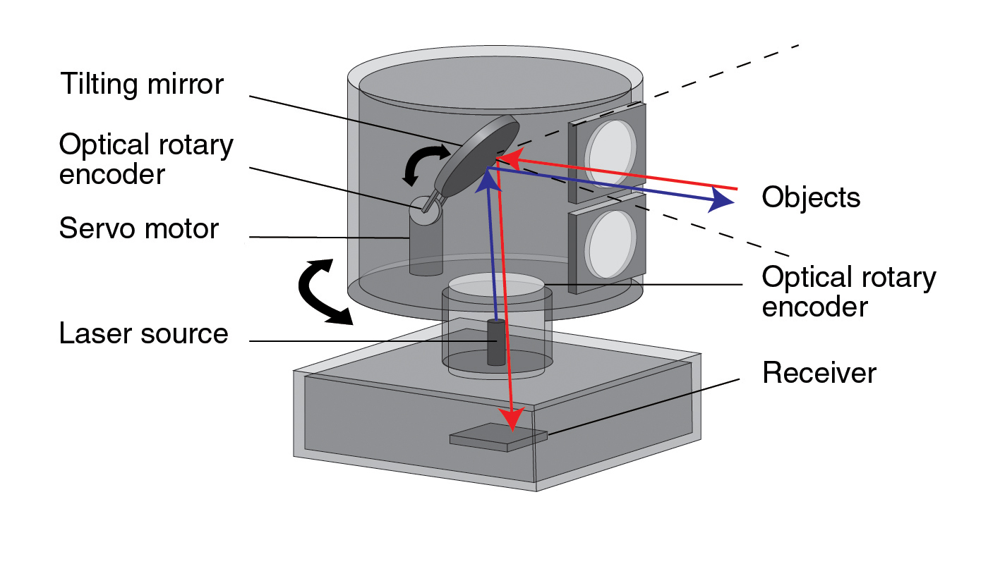
In addition to the transimitter (laser), the system requires a highly sensitive receiver. There are two gnereral trends in the automotive market now: infrared LIDAR systems that with the aid of a MEMS, use a rotating laser, or a solid-state LIDAR.

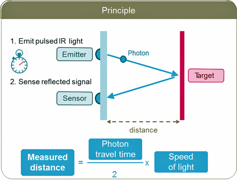
The receiving system has the task to recongnize the light beams emitted as well as reflected from the object. The detectors must be extremely  sensitive and able to measure single photons. Today, the state-of-the-art devices use SPAD technology.

The SPAD cell principle is simple. For the diode with a special geometry, the p-n junction is biased so that a single photon to trigger an avalanche breakdown current in the diode. The resulting sudden rise of the diode current is detected by a corresponding circuit, and then outputs the now digital signal for further processing. 

Image result for principle of lidar distance measurement

The principle of distance measurement is shown above using an SPAD sensor. The laser at t0 time emits a pulse which is reflected by the obstacle, and after t1 time one (or more) photon reaches the sensor cell. The distance can be determined from the running time.

If one or several beams are radiated by rotating mirrors or micro-mechanical systems and there is a correspondingly large pad array of several cells, three-dimension objects can be detected.


Fig. 13: Solid state lidar system
Solid state LIDAR system


Fig. 14: MEMS-based LIDAR system
MEMS-based LIDAR system

 Two common LIDAR systems are shown above. When using micro-mirror based on MEMS technology, the individual laser beam is radiated and reflected in a line shape. The reflected photons are evaluated by a corresponding optics sensor in the SPAD cell. Extreme demands are placed on the mirror system with regard to precision, service life, adjustablity, and reliability.

In this system, several laser diodes (over 100) and an accordingly large receiver array are required. The laser diodes must be equipped with pulse widths in the nanosecond range and with currents of a few amperes, which poses a significant challenge to the semiconductor drivers.

Most LiDAR systems employ infrared rather than visiable radiation. Because electromagnetic radiation's interaction with matter is governed by wavelength, some wavelengths work better for certain applications. Someday microwave (maser) or x-ray (xaser) lasers could be used to build LiDAR systems that can image through a wide variety of materials, greatly enhancing their usefulness.

Simplified block diagram of a D-TOF LiDAR system
Block diagram of a ToF LiDAR system (Image courtesy of ISSCC2018)

Solid-state LiDAR unites are on the market now. As time progresses, their cost will continue to drop and their capabilities will continue to improve. For example, it can be used from electric wheelchair and drones to motorcycles and other mobile plateforms, aside from autonomous cards.


Saturday, September 8, 2018

09-08-2018 open ASICedu blog


Today I opened the ASICedu blog.

I would like to share some excellent publications related to integrated circuit design such as phase-locked loop, A/D and D/A, time-to-digital converter, bandgap, high-speed I/O, operational amplifier, etc.

I would like to recommend some excellent IC reference books with some solutions and personal understandings.

I would like to post some interview questions to help people have a chance to get a nice job.

Having been an IC design engineer for several years, I used different PDKs and spent lots of time on learning different EDA tools. Hence, I would like to share some good solutions to setup the environment of EDA tools. I will also recommend some open source EDA tools.