Monday, September 24, 2018
Cadence APS vs XPS vs AMS
Cadence Spectre APS : Spectre Accelerated Parallel Simulator
Cadence Spectre XPS : Spectre eXtensive Partitioning Simulator
Cadence Spectre AMS Designer : Spectre AMS Designer Simulator
If you want to read the official documents about these three simulators, please visit cadence link.
You can also get a cadence tutorial file named: Spectre Circuit Simulator Reference from Cadence Support.
---
Spectre XPS is a FastSPICE circuit simulator that uses techniques like partitioning in order to simulate large, extracted netlists with 10's of millions of elements, and allowing IR drop analysis for extracted netlists.
Spectre APS is used for smaller designs and for highest accuracy circuits like: BER of an ADC, PLL jitter. It can be used without issues in transient analysis. (More discussions about APS, please email me.)
For introduction of AMS simulator, you can view ECEN 5007 course website of Prof. Hanh-Phuc Le.
Wednesday, September 12, 2018
LiDAR Introduction
In 2018, over $1B is raised by over 70 LiDAR companies. Analysts from Markets and Markets (www.marketsandmarkets.com) forecast the LiDAR market is going to hit 5,204.8 Million USD and will grow at a CAGR of 25.8% from 2018 to 2022. Therefore, the next five years will be a golden age for the automotive LiDAR market.
Today, let's talk about some basic knowledge about LiDAR.
LiDAR stands for Light Detection and Ranging (sometimes light imaging, detection, and ranging). It is a surveying method that measures a distance to a target by illuminating the target with pulsed laser light and measuring the reflected pulses with a sensor. Differences in laser return times and wavelengths can then be used to make digital 3-D representations of the target.
Applications
LiDAR has broad applications in geodesy, geomatics, archaeology, geography, geology, geomorphology, seismology, forestry, atmospheric physics, laser guidance, airborne laser swath mapping, and laser altimetry. Nowadays, it is also used in control and navigation for some autonomous cars becoming the world-wide favorite topic both in academic and industry.
If you would like to know more about history and general discussions about LiDAR, please visit LiDAR Wikipedia page.
 |
| Image of a rotating LiDAR unit from Renishaw. |
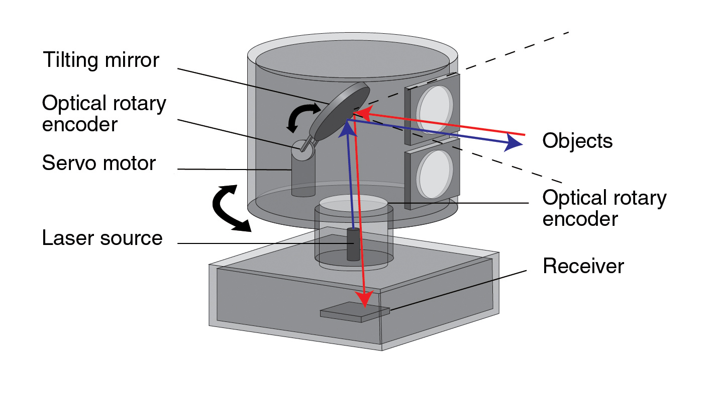
In addition to the transimitter (laser), the system requires a highly sensitive receiver. There are two gnereral trends in the automotive market now: infrared LIDAR systems that with the aid of a MEMS, use a rotating laser, or a solid-state LIDAR.
The receiving system has the task to recongnize the light beams emitted as well as reflected from the object. The detectors must be extremely sensitive and able to measure single photons. Today, the state-of-the-art devices use SPAD technology.
The SPAD cell principle is simple. For the diode with a special geometry, the p-n junction is biased so that a single photon to trigger an avalanche breakdown current in the diode. The resulting sudden rise of the diode current is detected by a corresponding circuit, and then outputs the now digital signal for further processing.
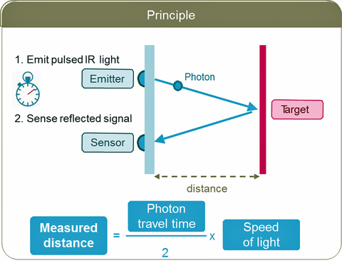
The principle of distance measurement is shown above using an SPAD sensor. The laser at t0 time emits a pulse which is reflected by the obstacle, and after t1 time one (or more) photon reaches the sensor cell. The distance can be determined from the running time.
If one or several beams are radiated by rotating mirrors or micro-mechanical systems and there is a correspondingly large pad array of several cells, three-dimension objects can be detected.
 | ||||||
| Solid state LIDAR system |
 |
| MEMS-based LIDAR system |
Two common LIDAR systems are shown above. When using micro-mirror based on MEMS technology, the individual laser beam is radiated and reflected in a line shape. The reflected photons are evaluated by a corresponding optics sensor in the SPAD cell. Extreme demands are placed on the mirror system with regard to precision, service life, adjustablity, and reliability.
In this system, several laser diodes (over 100) and an accordingly large receiver array are required. The laser diodes must be equipped with pulse widths in the nanosecond range and with currents of a few amperes, which poses a significant challenge to the semiconductor drivers.
Most LiDAR systems employ infrared rather than visiable radiation. Because electromagnetic radiation's interaction with matter is governed by wavelength, some wavelengths work better for certain applications. Someday microwave (maser) or x-ray (xaser) lasers could be used to build LiDAR systems that can image through a wide variety of materials, greatly enhancing their usefulness.
 |
| Block diagram of a ToF LiDAR system (Image courtesy of ISSCC2018) |
Solid-state LiDAR unites are on the market now. As time progresses, their cost will continue to drop and their capabilities will continue to improve. For example, it can be used from electric wheelchair and drones to motorcycles and other mobile plateforms, aside from autonomous cards.
Saturday, September 8, 2018
09-08-2018 open ASICedu blog
Today I opened the ASICedu blog.
I would like to share some excellent publications related to integrated circuit design such as phase-locked loop, A/D and D/A, time-to-digital converter, bandgap, high-speed I/O, operational amplifier, etc.
I would like to recommend some excellent IC reference books with some solutions and personal understandings.
I would like to post some interview questions to help people have a chance to get a nice job.
Having been an IC design engineer for several years, I used different PDKs and spent lots of time on learning different EDA tools. Hence, I would like to share some good solutions to setup the environment of EDA tools. I will also recommend some open source EDA tools.
Subscribe to:
Posts (Atom)