Saturday, December 16, 2023

QSPICE - Learn how to use QSpice from the beginning

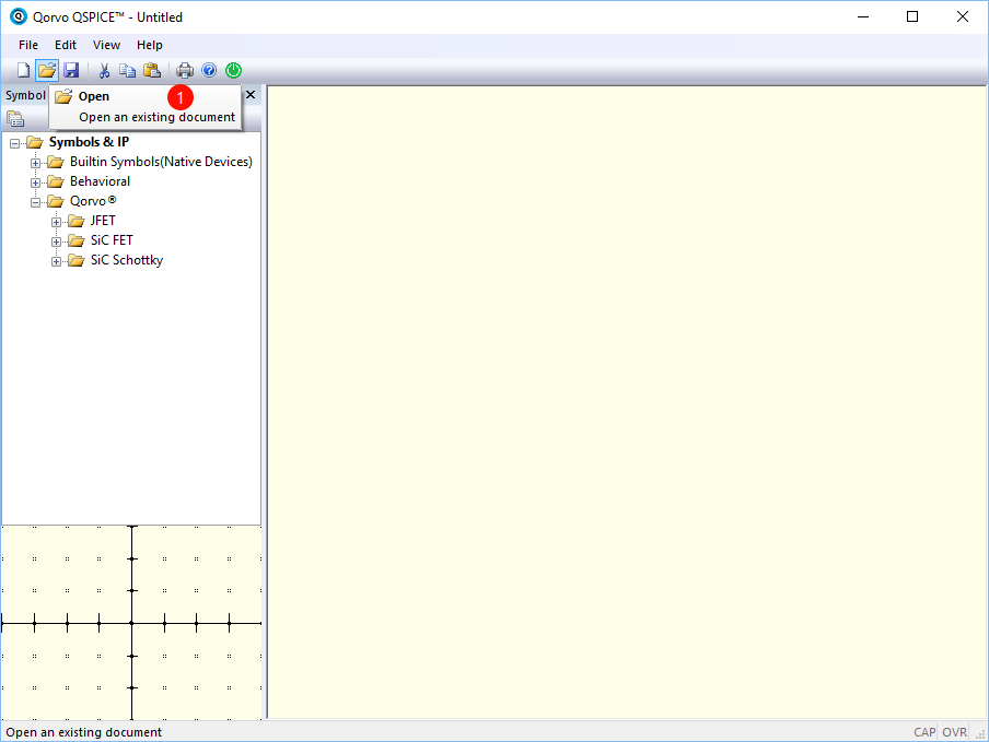
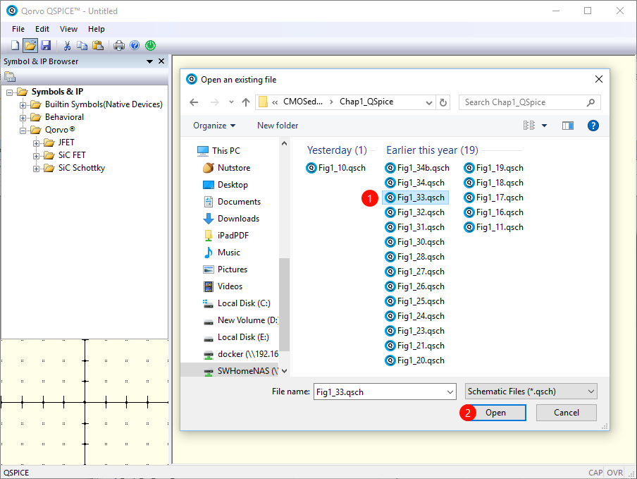
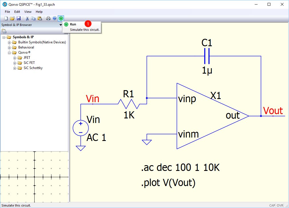
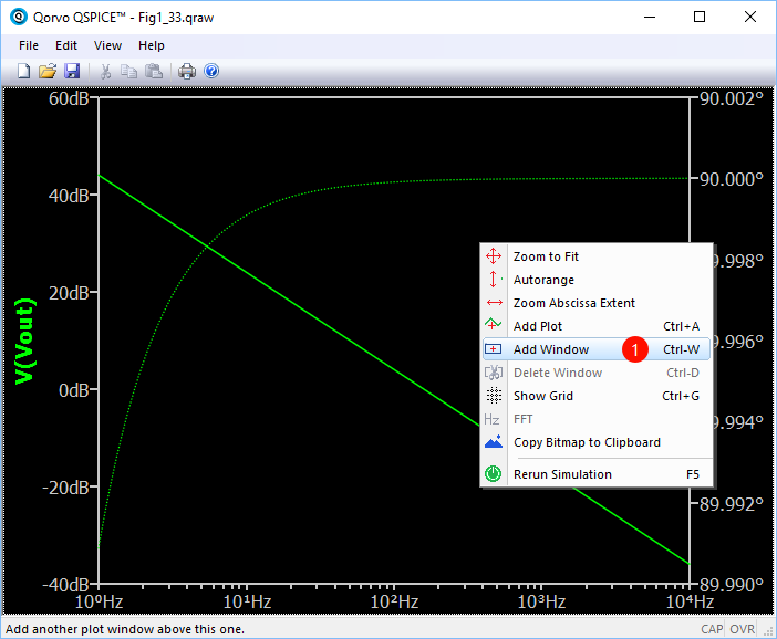
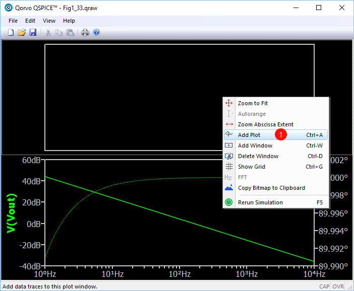
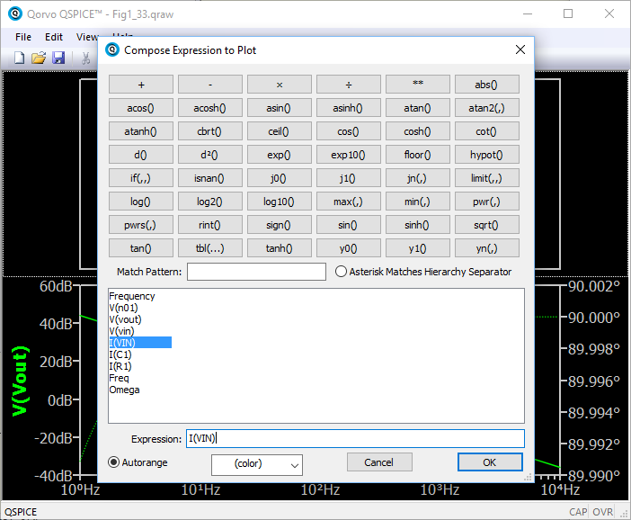
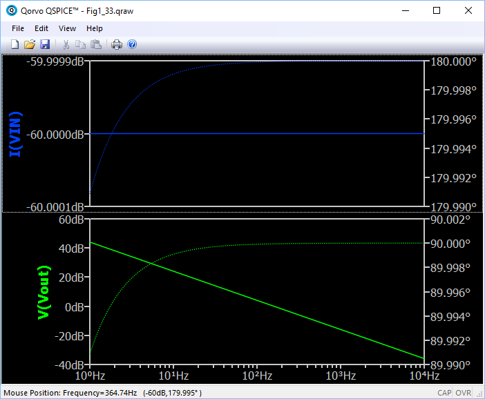
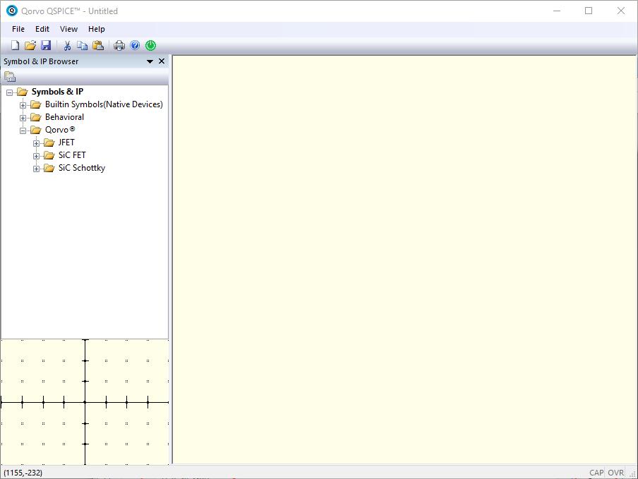
# Start to use Qspice textbook circuit models from ASICedu.com - Make sure to install QSPICE and unzip the Qspice_CMOSedu.zip (link) - Launch QSPICE - Open a schematic using the 'open' icon in the toolbar - Navigate to the Qspice model folder extracted from Qspice_CMOSedu.zip - Select a schematic corresponding to a book figure - Run the simulation by clicking the 'Green' icon in the toolbar menu - The simulation results will automatically plot in another Qspice window - To display some other signals, voltage or current: 1. make sure the '.save all' spice code is used in the schematic; 2. Right click the plot panel and select 'Add Window' to create a new panel; 3. Right click the new panel and select 'Add Plot' in the new panel; 4. Pick the voltage or current you like to plot and then click 'OK'. (On the top of 'Compose Expression to Plot', many math functions can be used) --- > Launch QSPICE image-20231216115834925 --- > Open a new QSPICE schematic image-20231216115938360 --- > Select the textbook circuit model image-20231216120058526 --- > Run the simulation image-20231216120236616 --- > Plot simulation results and Create a new window panel in the plot (Right click the current plot panel) ![image-20231216120703006](https://raw.githubusercontent.com/GalaxyGroot/imag4typora/main/2023/1216_12_08_41.png) --- > Add plot in the new panel (Right click the new panel) ![image-20231216120906887](https://raw.githubusercontent.com/GalaxyGroot/imag4typora/main/2023/1216_12_09_06.png) --- > Select another signal to plot in new panel and function table listed in the 'New Expression window' ![](https://raw.githubusercontent.com/GalaxyGroot/imag4typora/main/2023/1216_12_13_34.png) --- > Final Simulation Result Plot ![image-20231216121546282](https://raw.githubusercontent.com/GalaxyGroot/imag4typora/main/2023/1216_12_15_46.png)

Tuesday, December 12, 2023

Matlab - Add reference line in a bode plot

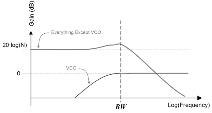
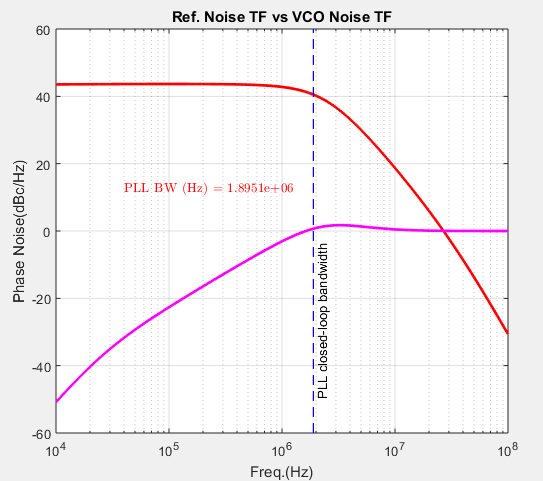
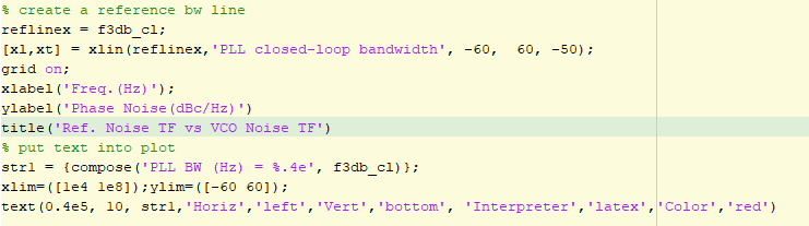
# Add reference line in a bode plot Sometimes, adding a reference line can explain a lot in a plot. For PLL noise transfer functions, the reference noise transfer function has a low pass characteristic. The VCO noise transfer function has a high pass characteristic. The PLL bandwidth splits the noise plot into two regions: - phase noise of VCO dominates the high frequencies because its noise transfer function have no effect in this region - phase noise of references and phase detector dominates the low frequency region image-20231211210530923 > noise transfer functions of the reference and VCO Therefore, it is useful to show the PLL bandwidth in the plot. New version Matlab provides a 'xline' function, vertical line with constant x-value, to plot a line in a plot. PixPin_2023-12-11_22-38-14 If you don't have the new version of Matlab, you can use another m function ([Link](https://wwem.lanzouq.com/iSonk1hpecmh)) to add a reference line. Example code is shown below: 122

Wednesday, November 29, 2023

Demo - IVerilog + GTKWave

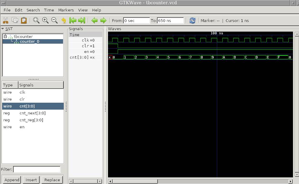
--- # Summary - installation iverilog and gtkwave - run the digital demo block to check the tool flow - compile the code: - `iverilog -o DUT.out DUT.v tb_DUT.v` - run the executable file - `vvp DUT.out` - plot dumped *.vcd* data file (don't forget the put dumped code in testbench) - `gtkwave DUT.vcd` - different OS can use different ways to make the flow easier. Please send an email to ask for codes working on Windows or Linux. - Window OS: `.bat` file - Linux OS: `Makefile` --- ``` initial begin $ dumpfile("DUT.vcd"); //The name of the generated vcd file $ dumpvars(0, tb_DUT ); //The name of the tb module end ``` --- # Introduction [Icarus Verilog](https://github.com/steveicarus/iverilog)) is an open-source Verilog simulator with _some_ SystemVerilog support. I really like to use it for quick digital circuit design and simulation. Icarus Verilog compiles the Verilog source into a file that is executed by its simulator `vvp`. [GTKWave](http://gtkwave.sourceforge.net/) is a open-source waveform viewer/plot tool, which is excellent for plotting digital signals in the simulation. It supports to read and view LXT, LXT2, VZT, FST, and GHW files as well as standard Verilog VCD/EVCD files Many fresh engineers might not be familiar with Iverilog and GTKWave. After using it for many years, I wish I know it when I was in college so I'd like to give a quick tutorial for all new engineer students who like to try open-source digital tool. # Demo Example Basic 4-b counter is written in verilog. ``` /** * 4-bit counter */ module counter ( input clk, // posedge clock input clr, // synchronous clear input en, // enable: active high to increment output [3:0] cnt // counter value ); reg [3:0] cnt_reg, cnt_next; assign cnt = cnt_reg; always @(*) begin cnt_next = cnt_reg; if (clr) begin cnt_next = 4'd0; end else if (en) begin cnt_next = cnt_reg + 1; end end always @(posedge clk) begin cnt_reg <= cnt_next; end endmodule ``` The simple counter testbench ``` `timescale 1ns/100ps // 1 ns time unit, 100 ps resolution module tb_counter; reg clk; always #5 clk = !clk; reg clr, en; wire [3:0] cnt; counter counter_0 ( .clk(clk), .clr(clr), .en(en), .cnt(cnt) ); integer i; initial begin // create a VCD waveform dump called "tb_counter.vcd" // dump variable changes in the testbench // and all modules under it $dumpfile("counter.vcd"); $dumpvars(0, tb_counter); end initial begin $monitor("t=%-4d: cnt = %d", $time, cnt); clk = 0; clr = 1; en = 0; @(negedge clk); clr = 0; en = 1; for (i = 0; i < 64; i = i + 1) begin @(negedge clk); end $finish(); end endmodule ``` The function `$dumpfile()` and `$dumpvars()` are to output vcd file for plotting data. # Simulation Flow ## compile and run iverilog compiles the source modules to produce files for vvp. ``` iverilog -o tb_counter.out counter.v tb_counter.v vvp counter.out ``` Makefile is used to speed up in Linux. ``` TOP = test_counter SRC = counter.v TEST_SRC= tb_counter.v BIN = $(TOP).vvp $(BIN): $(SRC) $(TEST_SRC) iverilog -o $(BIN) -s $(TOP) $(SRC) $(TEST_SRC) .PHONY: all clean test all: $(BIN) test: $(BIN) vvp $(BIN) clean: rm -f *.vvp *.vcd ``` For better usage, I have an updated Makefile. Please send me an email to get a copy of it. ## Plot Data GTKWave is to open vcd files and to plot signals. ``` gtkwave counter.vcd ``` # More about Iverilog ## parameter `-o` set the name of compiling output file: `iveirlog test.v -o test.out` ## parameter `-y` set the project folder or design folder: `iverilog -y $DIR/demo demo_tb.v` ## parameter `-tvhdl` convert verilog to VHDL: `iverilog -tvhdl -o output_file.vhd in_file.vhd`

Wednesday, November 9, 2022

Creating Device Sue Symbols for SkyWater SKY130 Process

I customized device symbols for using CppSim/Sue tool to run skywater sky130 process.

CppSim is an open-source, wonderful and powerful EDA tool. I like to use it for running some simulations. In order to design circuits in real PDK, I start this interesting project.

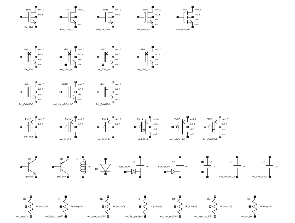
Now I listed the following symbols ready to use.


image-20221109205824822


The following demo is shown to demonstrate a simple circuit simulation flow by using sue+ngspice+sky130_pdk.


image-20221109210734483

image-20221109210650828

Tuesday, January 25, 2022

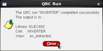
Cadence QRC notes

Cadence QRC notes

Cadence QRC is the parasitic RCL (resistance, capacitance, and inductance) extraction tool which is valuable and powerful to help IC designers to complete both digital- and transistor-level circuit design and assure on-time tapeout.

img

Correct QRC Tips

Several useful tips can assure engineers to run efficiently and faultless:

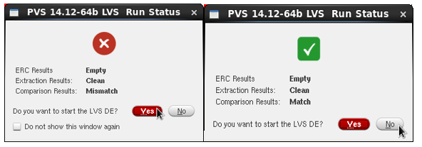
  1. Pass the LVS check before proceeding

    img

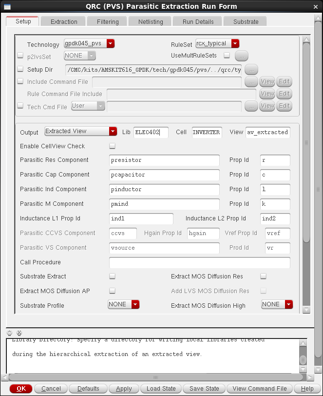
  2. Select the correct Setup Dir to the PDK QRC folder if RuleSet is displayed 'NONE'. (different QRC setup dir: RC, RC_type, RC_max, RC_min, etc. ) In typical, select RC_max QRC folder to get the worse case result.

  3. Set different Temperature in Extraction option. In the PVT simulation, engineers usually are asked to run TT 27C, FF -40C, SS 125C for pre- and post-simulation. So several extraction views are generated like av_extracted_rcmax_27, av_extract_rcmax_125, av_extract_rcmax_n40.

  4. Set Ref Node to be the correct ground PIN of the design block

  5. Set Extraction Type to be RC or C only typically

  6. Enter all PIN names of VDDs and Grounds to the Power Nets and Ground Nets in the Filtering option


Final Correct Window of QRC extraction

img


Parasitic back-annotation

After getting the parasitic extraction cell view, check/review the parasitics in schematic view could help engineers to understand which nodes have more parasitics.

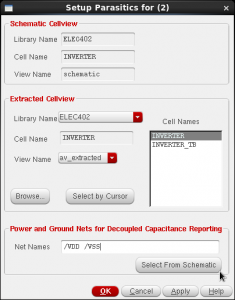
Back-annotation tool can be launched in schematic window by clicking Launch ---> Plugins ---> Parasitics. In Setup Parasitics window as below, make sure select the correct view name and cell name. Then, press OK and go to Parasitics Menu to select Show Parasitics.

Figure 18 Setup Parasitics.

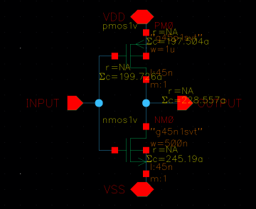
The original schematic displays the summation of capacitance in each node.

Figure 19 CMOS inverter with the annotated parasitic capacitance.

Post-simulation

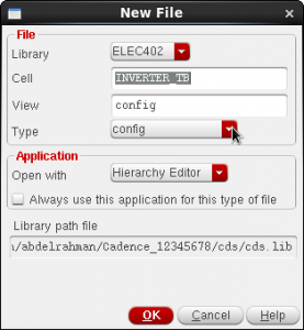
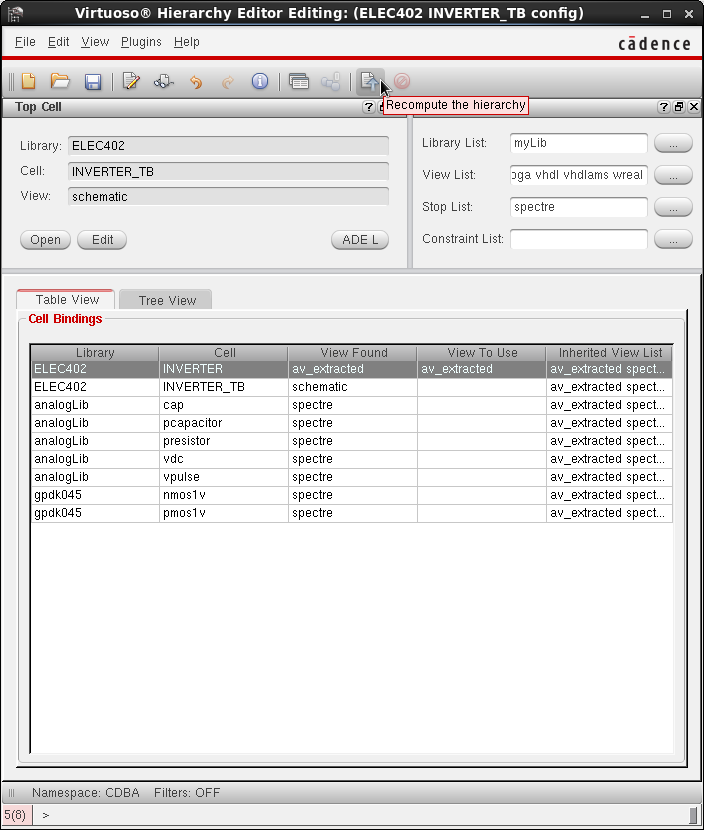
Post-simulation process needs to create the 'config' view of the testbench cell and then select the extraction cell view of expected subcircuits or the whole top-level design.

In the New Configuration window, please use AMS temperate for mixed-signal circuit simulation, which means the testbench has some block in verilog/verilogams models.

Figure 20 Create config view for the TB.

In the expected checking circuit, select its extraction view. Better to update or recompute the hierarchy to proceed the simulation process.

Press Open to open the schematic editor with the config view and launch ADE L or ADE XL or ADE explorer to run the simulation.

Tips:

  1. Select the design block and Press 'E' to check what is the current cell view. It should be matched to the view in the config window
  2. always make sure that the word 'config' exists in the schematic editor window's name
  3. update and recompute the hierarchy whenever the schematic is modified or check and saved

img

Thursday, June 24, 2021

design procedure for ADPLL parameter determination

System design procedure for Type-II second-order ADPLL 

Reading the following reference, learn how to analyze the ADPLL. There is an error in calculating the resistor of the loop filter. It was corrected in the matlab code.

[1]
V. Kratyuk, P. K. Hanumolu, U.-K. Moon, and K. Mayaram, “A Design Procedure for All-Digital    Phase-Locked Loops Based on a Charge-Pump Phase-Locked-Loop Analogy,” IEEE Transactions on Circuits and Systems II: Express Briefs, vol. 54, no. 3, pp. 247–251, Mar. 2007, doi: 10.1109/TCSII.2006.889443.

For better learning and understanding the publication, I created a mindmap reference and matlab code. 

  • Mindmap Reference and Matlab code: Download Link (send email to me to ask for the password)


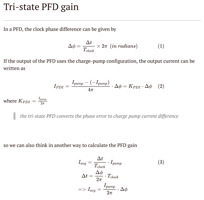
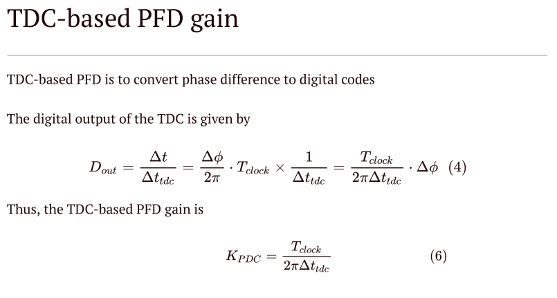
PFD gain calculation

image-20210706104130460


image-20210706104145548

Monday, June 7, 2021

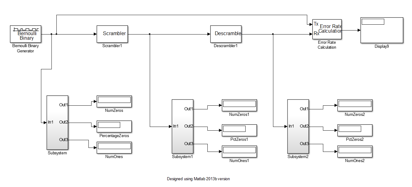
Simulink model of Scrambler and Descrambler

Scrambler often referred as randomizer basically removes long stream of zeros and ones from the data. It is used in wireless transmitter and receiver chain. Descrambler is the reverse operation.

image-20210607220054668

Link: https://wwr.lanzoui.com/iwlVxpxtk6d

Zip file is password protected. Please send an email to asic at asicedu.com for asking.

Thursday, June 3, 2021

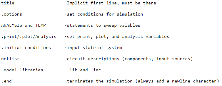
HSCPIE Files Explanation

HSPICE Major Files Explanation

Input files:

  1. netlist source: filename.sp
  2. initialization: hspice.ini
  3. design configuration: filename.cfg

Output files:

  • run status: filename.st0
  • output listing: filename.lis
  • graph data files
gRAPH DATAANALYSIS RESULT
*.tr0transient
*.sw2dc
*.ac1ac

in general, you only need to know about some of these files: source file, output listing, and graph data.


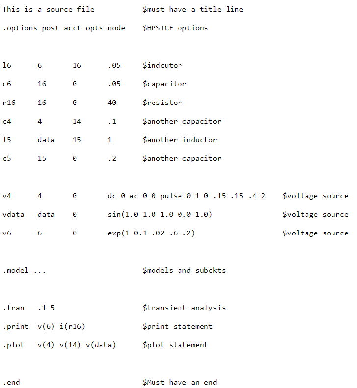
source file (.sp)

The source file contains your circuit description and all options and analysis setup.

image-20210603122255308


For example:

image-20210603122319480

Output listing(.lis)

This is one of the most important files in HSPICE as this file lists all results obtained from the simulation. This file contains (in order of listing in the file):

  • HSPICE licensing information
  • Listing of the circuit
  • Results form the analysis of the circuit (.op, .print, .plot, .measure, .ac, and .tran in order of their appearance in the source file)

reference: Files (columbia.edu)

Friday, November 13, 2020

charge pump non-ideal design consideration

The practical design issues in PLLs related to the charge pump block is the unbalanced large-signal operation that transforms the timing information or phase difference information to analogue quantity in voltage to control the VCO. 

Three different design considerations for PFD+CP noise performance:

- leakage current of Charge Pump: the reference spur caused by the leakage current is possibly substantial in frequency synthesizers. (If the spur level is not enough to meet the requirement, the loop bw should be further narrowed or the charge pump current should be increased. Note: reducing the division value by increasing the frequency frequency like fractional-N frequency synthesizers is very helpful to relax the charge pump design.)

- mismatches in Charge Pump: CP mismatch has two factors: one is the current mismatch, the other is the switching-on time mismatch of UP/DOWN operations. When the mismatch is given in the charge pump, it is important to reduce the turn-on time of the PFD that is equivalent to the minimum pulse width of the output to avoid the dead-zone. 

- timing mismatch in PFD: timing mismatch is inherent in PFD with the single-ended charge pump since the UP/DOWN outputs have to drive PMOS and NMOS switches. (When delay mismatch is much smaller than the turn-on time of PFD, the timing mismatch issue is less significant compared to the leakage current or the mismatch in the charge pump.)

Wednesday, November 11, 2020

Different Extraction Tools

For IC design, different extraction tools can be used to generate the post-layout netlist.

  • StarRC - from Synopsys
  • Quantus QRC - from Cadence
  • Calibre xRC - from Mentor Graphics

Noise discussion in PFD/CP

The two noise contributions in the PFD/CP:

  • PFD jitter
  • noise in the output current of the CP

The PFD noise will all be in the charging and discharging edges and will be independent of how long the CP is on. However, the total noise produced by the CP will be proportional to how long it is on.

Two current sources provided to loop filter by the CP: one is pull-up current and the other pull-down current. Which one is activated depends on whether the edges on the reference input lead or lag those on the feedback input signal. When edges from PFD or UP/DOWN signals occur simultaneously, both the pull up and pull down current sources will turn on for a very short period of time. From an output current perspective the pull up and pull down currents will act to cancel each other and so the effective output current is zero. (If the current is not zero, what happens?)

And both current sources will be contributing uncorrelated noise (“Uncorrelated” means that the values are independent; that is, knowing one value provides no information about the others.) to the output while they are on. Thus, it is best to characterize the noise of the PFD/CP with simultaneous edges occurring on both the reference and feedback inputs. The output should be connected to a current probe (ideal voltage source) that is biased to present the expected voltage to the output of the CP.

Using Cadence PSS+Pnoise analysis, the phase noise of the PFD/CP can be obtained. Which is the right sweep type correct: relative or absolute?

If setting the sweep type= relative, the actual sweeping frequency is f1+n*Fpss to f2+n*Fpss, where f1 and f2 are the defined sweeping range and n is the relative harmonic number, Fpss is the PSS fundamental frequency. The benefits of the relative sweep is when simulating oscillators, because you want to look at the noise skirts around the oscillator frequency, but you don't know the oscillator frequency (accurately enough) before running, so letting PSS find it itself, and doing a relative sweep makes sense.

What about absolute sweep?

Recommended operational amplifier (opamp) reference books

 Design of Low-Voltage Low-Power Operational Amplifier Cells

- Written by Ron Hogervost and Johan Huijsing


Introduction to CMOS Opamps and Comparators

- Written by Roubik Gregorian


Operational Amplifiers -Theory and Design 

- Written by Johan H. Huijsing


Analog Integrated Circuit Design 

- Written by David Johns and Ken Martin

Tuesday, November 3, 2020

Cadence ViVA Commonly-Used Keybindings

RMB = right mouse buttom

MMR = middle mouse roll


Function

Bindkey

Zoom in

RMB-drag box or ]

Zoom out

[

Zoom in X

Shift-RMB-drag or X (RMB-drag) or Shift-MMR

Zoom in Y

Ctrl-RMB-drag or Y (RMB-drag) or Ctrl-MMR

Zoom Full or Fit into window

F

Undo

U

Pan

Arrow keys or Ctrl-Alt-RMB

Edit Properties

Q

Trace Cursor

C (toggle)

Horizontal Marker

H

Vertical Marker

V

A/B Marker

A/B

Point Marker

M

Delta Marker

D

Rise/Fall Time Marker

T

Reference Point Marker

R

Delete

Delete

Delete All

E

Delete All Markers

Ctrl-E

Snap Markers to Previous/Next

P/N

Cut

Ctrl-X

Copy

Ctrl-C

Paste

Ctrl-P

Select All traces in strip

Ctrl-A

Select All traces in subwindows

Shift-Ctrl-A

Create New Window

Ctrl-N

Reload Current subwindow

Ctrl-R


Wednesday, August 19, 2020

Wide Dynamic Range TDC 2015-TCASII Paper 8/2020

Publication Title: A_Wide_Range_42_psrms_Precision_CMOS_TDC_With_Cyclic_Interpolators_Based_on_Switched-Frequency_Ring_Oscillators


The publication obtained a 327us measurement range with a main reference clock counter and two interpolators. The design method is based on Nutt interpolation.
nutt interpolation figure

The introduction was excellent to teach us to learn about the TDC background. Although TDCs are used in ADPLLs as a phase detector, the paper focused on its another application: time-of-flight applications. That means the wide-range TDC is used to measure distance with a few hundred kHz clock rate.

Personally, I really like the rest of the introduction to discuss different types of TDC. Flash type TDCs using delay lines or ring oscillators have a nonlinearity issue caused by the delay mismatch and threshold mismatch. The vernier delay line improves the TDC resolution by subtracting two delay values. However, for the same measurement range, the vernier delay TDCs need longer delay units than the flash type TDCs. And also the random jitter increases as the delay line increases. Both of them is sensitive to PVT variations.

The third type of TDC is gated ring oscillator type. It provides a 1st order noise shaping. Without reseting for every step quantization, the current phase information is retained for next quantization cycle. After differentiation, the phase error or quantization error is noise-shaped.

In addition, the pipeline, cyclic, SAR TDCs are designed with a time difference amplifiers. However, the dynamic range of them is limited.

In sum, all these TDCs can be divided to short-range and long-range. Short range TDCs could get higher resolution. However, counter-based TDCs for long range measurements needs a fast clock to obtain a good resolution.

Thus, the paper proposed a combination method (Nutt interpolation) of using a main-counter TDC dealing with long range measurement and using high resolution TDCs to measure the interpolator range. So this type of TDC can achieve both high range and high resolution.

The advantages:
1. High range + high resolution
2. The input signal is asynchronous with respect to the reference clock so the linearity of the TDC can be improved by asynchronous input scrambles all the interpolators errors.

The major design discussion of the publication focused on the ring-oscillator TDC with two frequencies to amplifier the time residue, which is called switch-frequency ring oscillator. Furthermore, a digital calibration method is introduced for radix extraction.

Two points are good to know:
1. Real circuit needs a input generator block to generate the start and stop signals
2. DFF metastability issue could happen when start/stop edge coincide with the reference clock edge. Two DFFs are used to relieve the metastability.
3. The interpolator nonlinearity doesn't mean the whole TDC is nonlinear. The static nonlinearity of the TDC depends on the relation between the reference clock and the start signal.


By asicedu.com
Monday, June 10, 2019

RMS to Peak-to-Peak Jitter conversion

RMS to Peak-to-Peak Jitter conversion

RMS to Peak-to-Peak Jitter conversion

To converter between RMS and peak-to-peak random jitter, the bit-error-rate (BER) must be specified.


where is determined by

The following table is to depict the scaling factor for different BER.

BER vs alpha

If some one wants to save a copy of the table to his or her personal computer, please click the link to download: google sheet link.

RMS noise value of comparator

The comparator offset is mean value of output normal distribution. RMS noise value is the one standard deviation of the normal distribution.

For an error rate , the input must exceed the input offset by up and down times the RMS noise level. For example, the offset of an comparator is . The RMS noise is , so the high output logic level the required input voltage is . For the low output logic level, the input must be below .