Cadence QRC notes
Cadence QRC is the parasitic RCL (resistance, capacitance, and inductance) extraction tool which is valuable and powerful to help IC designers to complete both digital- and transistor-level circuit design and assure on-time tapeout.
Correct QRC Tips
Several useful tips can assure engineers to run efficiently and faultless:
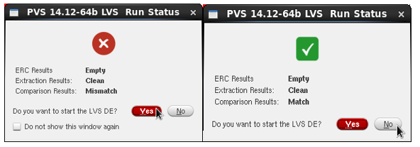
Pass the LVS check before proceeding
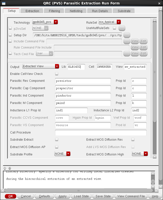
Select the correct Setup Dir to the PDK QRC folder if RuleSet is displayed 'NONE'. (different QRC setup dir: RC, RC_type, RC_max, RC_min, etc. ) In typical, select RC_max QRC folder to get the worse case result.
Set different Temperature in Extraction option. In the PVT simulation, engineers usually are asked to run TT 27C, FF -40C, SS 125C for pre- and post-simulation. So several extraction views are generated like av_extracted_rcmax_27, av_extract_rcmax_125, av_extract_rcmax_n40.
Set Ref Node to be the correct ground PIN of the design block
Set Extraction Type to be RC or C only typically
Enter all PIN names of VDDs and Grounds to the Power Nets and Ground Nets in the Filtering option
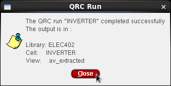
Final Correct Window of QRC extraction
Parasitic back-annotation
After getting the parasitic extraction cell view, check/review the parasitics in schematic view could help engineers to understand which nodes have more parasitics.
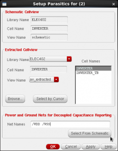
Back-annotation tool can be launched in schematic window by clicking Launch ---> Plugins ---> Parasitics. In Setup Parasitics window as below, make sure select the correct view name and cell name. Then, press OK and go to Parasitics Menu to select Show Parasitics.
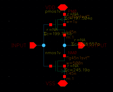
The original schematic displays the summation of capacitance in each node.
Post-simulation
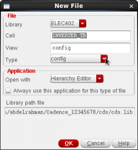
Post-simulation process needs to create the 'config' view of the testbench cell and then select the extraction cell view of expected subcircuits or the whole top-level design.
In the New Configuration window, please use AMS temperate for mixed-signal circuit simulation, which means the testbench has some block in verilog/verilogams models.
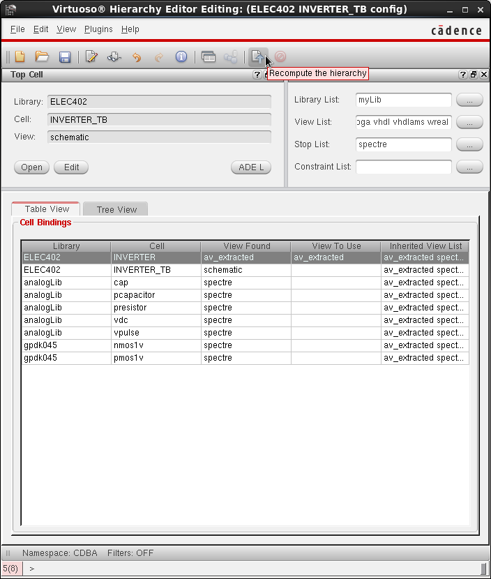
In the expected checking circuit, select its extraction view. Better to update or recompute the hierarchy to proceed the simulation process.
Press Open to open the schematic editor with the config view and launch ADE L or ADE XL or ADE explorer to run the simulation.
Tips:
- Select the design block and Press 'E' to check what is the current cell view. It should be matched to the view in the config window
- always make sure that the word 'config' exists in the schematic editor window's name
- update and recompute the hierarchy whenever the schematic is modified or check and saved
 ---
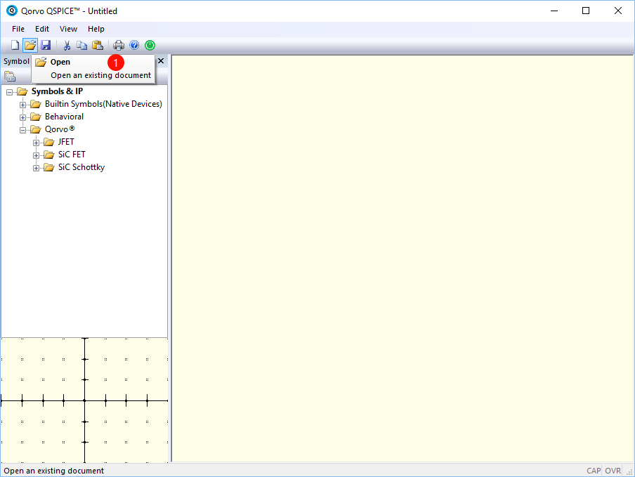
> Open a new QSPICE schematic
---
> Open a new QSPICE schematic
 ---
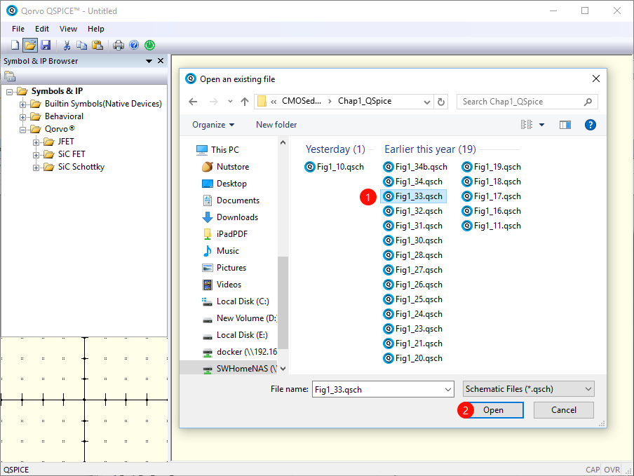
> Select the textbook circuit model
---
> Select the textbook circuit model
 ---
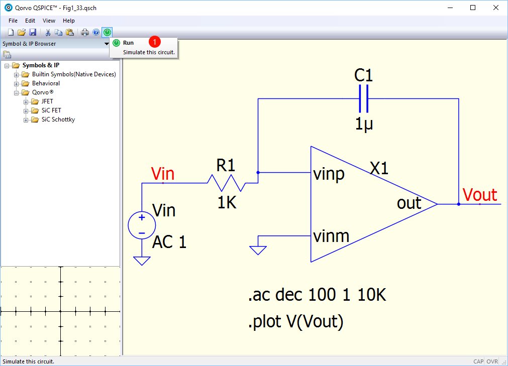
> Run the simulation
---
> Run the simulation
 ---
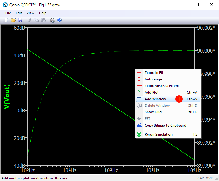
> Plot simulation results and Create a new window panel in the plot (Right click the current plot panel)
---
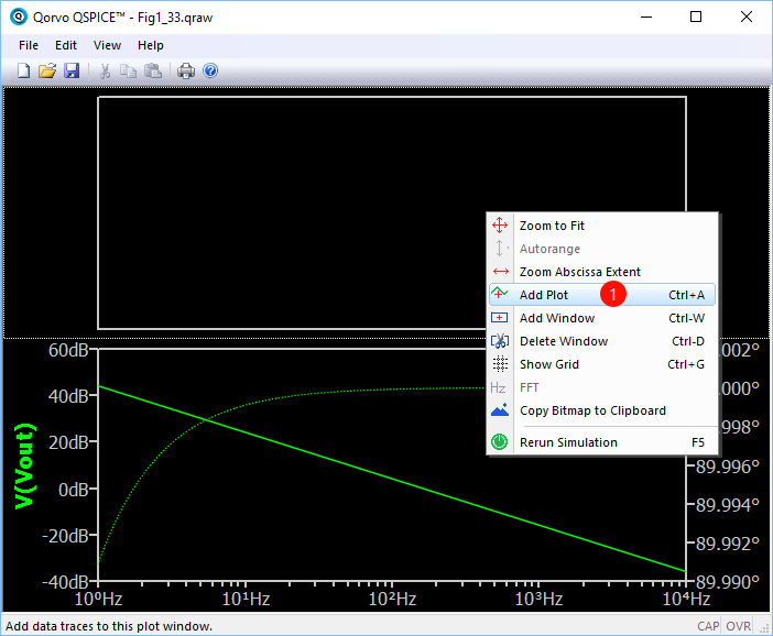
> Add plot in the new panel (Right click the new panel)
---
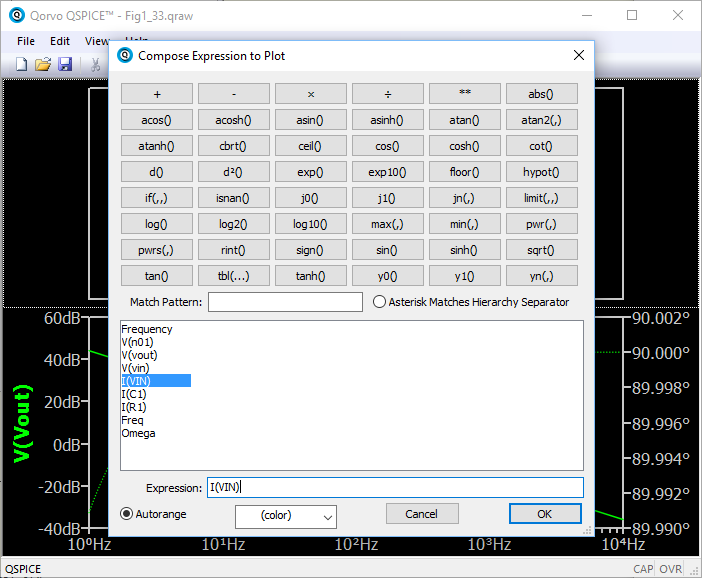
> Select another signal to plot in new panel and function table listed in the 'New Expression window'
---
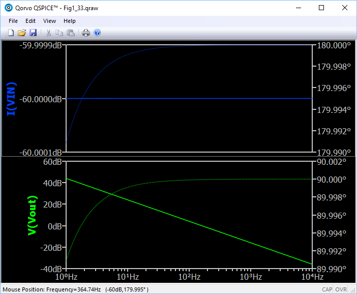
> Final Simulation Result Plot
---
> Plot simulation results and Create a new window panel in the plot (Right click the current plot panel)

---
> Add plot in the new panel (Right click the new panel)

---
> Select another signal to plot in new panel and function table listed in the 'New Expression window'

---
> Final Simulation Result Plot

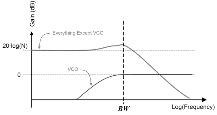 > noise transfer functions of the reference and VCO
Therefore, it is useful to show the PLL bandwidth in the plot.
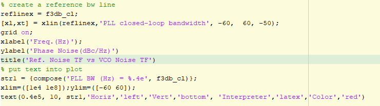
New version Matlab provides a 'xline' function, vertical line with constant x-value, to plot a line in a plot.
> noise transfer functions of the reference and VCO
Therefore, it is useful to show the PLL bandwidth in the plot.
New version Matlab provides a 'xline' function, vertical line with constant x-value, to plot a line in a plot.
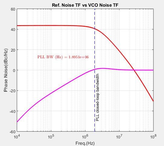 If you don't have the new version of Matlab, you can use another m function ([Link](https://wwem.lanzouq.com/iSonk1hpecmh)) to add a reference line.
Example code is shown below:
If you don't have the new version of Matlab, you can use another m function ([Link](https://wwem.lanzouq.com/iSonk1hpecmh)) to add a reference line.
Example code is shown below:
 # More about Iverilog
## parameter `-o`
set the name of compiling output file: `iveirlog test.v -o test.out`
## parameter `-y`
set the project folder or design folder: `iverilog -y $DIR/demo demo_tb.v`
## parameter `-tvhdl`
convert verilog to VHDL: `iverilog -tvhdl -o output_file.vhd in_file.vhd`
# More about Iverilog
## parameter `-o`
set the name of compiling output file: `iveirlog test.v -o test.out`
## parameter `-y`
set the project folder or design folder: `iverilog -y $DIR/demo demo_tb.v`
## parameter `-tvhdl`
convert verilog to VHDL: `iverilog -tvhdl -o output_file.vhd in_file.vhd`